Walk into any modern electronics lab, open up a smartphone, or inspect a solar panel — and you’ll find semiconductors at the heart of the action. These materials are the foundation of all modern electronic devices, enabling all from switching operations to data storage, light release, and energy harvesting.
But at the root of this amazing technology lie two fundamental groups: intrinsic and extrinsic semiconductors.
In this post, we’ll explore:
- What these two types are
- How they’re different (and why that matters)
- Their electrical properties
- How doping changes everything
- Real-world examples where they’re used
Let’s clarify the science and discover why semiconductors are the engine of modern electronics.
🧪 What Are Semiconductors?
A semiconductor is a material that has electrical conductivity between that of a conductor (like copper) and an insulator (like glass). Their unique behavior allows them to conduct electricity under certain conditions, making them perfect for creating transistors, diodes, LEDs, and combined circuits.
Semiconductors are mostly made from silicon (Si), although germanium (Ge) and gallium arsenide (GaAs) are also common in special applications.
🔍 Intrinsic vs. Extrinsic Semiconductors — What’s the Difference?
At the core, the difference comes down to purity and modification.
| Type | Description | Example |
| Intrinsic | Pure semiconductor with no added elements | Pure silicon |
| Extrinsic | Semiconductor that has been doped with impurities to change its properties | Silicon doped with phosphorus (n-type) or boron (p-type) |
Let’s dig into each of them in detail.
🌱 Intrinsic Semiconductors
Intrinsic semiconductors are pure materials, free from any significant impurities. The most common inherent semiconductors are pure silicon (Si) and germanium (Ge).
At absolute zero (0 K), these materials behave like perfect insulators. But at room temperature, thermal energy excites some electrons, allowing them to jump from the valence band to the conduction band — allowing a small amount of conductivity.
🧬 Band Theory and Charge Carriers
In intrinsic semiconductors:
- Electrons jump to the conduction band, leaving behind holes in the valence band.
- Both electrons and holes contribute equally to conduction.
So, number of electrons (n) = number of holes (p) in intrinsic semiconductors.
This relationship is given by:
n = p = ni
Where ni is the intrinsic carrier concentration.
🔋 Electrical Properties of Intrinsic Semiconductors
- Low conductivity compared to metals
- Resistivity decreases with rising temperature (opposite of metals)
- Balanced carrier population
- No doping — natural charge carriers
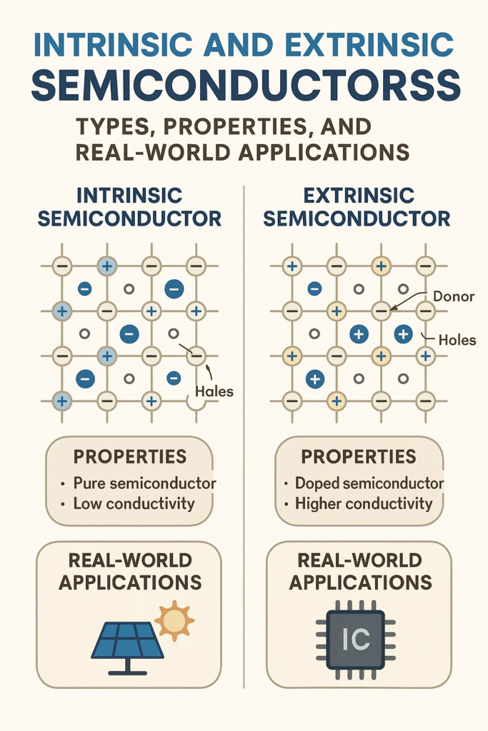
🧪 Extrinsic Semiconductors
An extrinsic semiconductor is a doped version of an intrinsic semiconductor. By intentionally adding small amounts of impurities, we can radically change the material’s conductivity and behavior.
The process of adding these impurities is called doping.
Types of Extrinsic Semiconductors
There are two types, based on the type of impurity added:
⚡ 1. N-Type Semiconductor (Negative-Type)
- Created by doping silicon or germanium with pentavalent atoms (elements with 5 valence electrons), such as:
- Phosphorus (P)
- Arsenic (As)
- Antimony (Sb)
These extra atoms donate a free electron, collective electron concentration.
Key features:
- Electrons are the majority charge carriers
- Holes are the minority
- Conductivity is higher than intrinsic material
n >> p
🔴 2. P-Type Semiconductor (Positive-Type)
- Made by doping with trivalent atoms (3 valence electrons), such as:
- Boron (B)
- Gallium (Ga)
- Indium (In)
These create holes in the crystal structure (missing electrons), which act as positive charge carriers.
Key features:
- Holes are the majority carriers
- Electrons are the minority
- Also highly conductive
p >> n
⚙️ How Doping Affects Semiconductor Behavior
Adding dopants (typically in attentions like 1 atom per million silicon atoms) has a massive effect on electrical behavior.
Key impacts:
- Increased conductivity by 100 to 100,000 times
- Ability to control current direction (crucial for diodes and transistors)
- Creation of p-n junctions, the building blocks of all modern electronics
Doping turns silicon from a weak conductor into a programmable electronic material — making the microchip rebellion possible.
🧰 Properties Comparison Table
| Property | Intrinsic | N-Type | P-Type |
| Doping | None | Pentavalent atoms | Trivalent atoms |
| Majority carriers | Electrons = Holes | Electrons | Holes |
| Minority carriers | — | Holes | Electrons |
| Conductivity | Low | High | High |
| Temperature response | Conductivity increases with temperature | Same | Same |
🌎 Real-World Applications
Let’s explore how intrinsic and extrinsic semiconductors are used in practical electronics and energy systems.
📱 1. Transistors (BJT, MOSFET)
These are the core components in almost every electronic device.
- Made by combining p-type and n-type semiconductors in a specific structure
- Used for switching, amplifying, and processing signals
Your computer, smartphone, and TV wouldn’t work without them.
🔌 2. Diodes (Rectifiers, LEDs, Zeners)
Diodes are two-terminal components made from a p-n junction.
- Used to allow current flow in one direction
- In LEDs, electrons and holes recombine to emit light
- In Zener diodes, opposite breakdown is used for voltage regulation
⚡ 3. Solar Cells (Photovoltaics)
Solar cells are p-n junctions bare to sunlight.
- Photons knock electrons moveable, generating electric current
- Used in rooftop panels, solar-powered lights, spacecraft, and more
These rely on precisely engineered doping to enhance energy conversion.
🔋 4. Thermistors and Temperature Sensors
Intrinsic semiconductors like germanium and silicon are used in thermistors.
- Their resistance changes probably with temperature
- Used in climate control, engine monitoring, medical devices
🚗 5. Electric Vehicles and Power Electronics
Power MOSFETs and IGBTs (insulated gate bipolar transistors) used in EVs are built using heavily doped extrinsic semiconductors for high efficiency.
- Control motor speed
- Manage battery charging
- Convert between AC and DC
🧠 6. Integrated Circuits (ICs)
All from microcontrollers to microprocessors is made using millions or billions of transistors on a chip — each one built from extrinsic semiconductors.
- Logic gates
- Memory storage
- Clock generation
All are possible because of p-n junction engineering.
🧬 Physics Behind the Magic
To really understand how semiconductors work, you should know about:
1. Energy Band Gap
- Conductors: No gap between valence and conduction bands
- Insulators: Large gap
- Semiconductors: Medium band gap (1.1 eV for silicon)
This small gap means thermal or visual energy can excite electrons into conduction.
2. Drift and Diffusion Currents
In semiconductors, current flows in two ways:
- Drift: Caused by an electric field
- Diffusion: Caused by concentration differences
Devices like diodes and solar cells rely on this dual behavior.
3. Recombination and Generation
- Electrons can recombine with holes, releasing energy (e.g., in LEDs).
- New carriers are generated thermally or optically.
Control over these processes defines the behavior of semiconductor devices.
🔮 Future Trends in Semiconductor Materials
While silicon dominates, other materials are growing in admiration for specific applications:
1. Gallium Nitride (GaN)
- Higher efficiency and speed than silicon
- Used in fast chargers, 5G, and radar systems
2. Silicon Carbide (SiC)
- Great for high voltage and temperature
- Used in EVs, solar inverters, and aerospace
3. Organic Semiconductors
- Flexible and printable
- Found in flexible screens and wearable electronics
❓ Frequently Asked Questions
Q1: Can intrinsic semiconductors be used in real circuits?
Rarely. Their conductivity is too low. They’re mainly used in controlled experiments or as the base for doping.
Q2: Is doping reversible?
No. Once doped, a semiconductor’s structure is permanently changed.
Q3: Can we combine n-type and p-type materials?
Yes — that’s how we make diodes, transistors, and solar cells!
Q4: Are semiconductors only used in electronics?
No. They’re also used in medical imaging, solar panels, sensors, and quantum research.
🧾 Conclusion
Intrinsic and extrinsic semiconductors may seem like nonconcrete physics terms, but they’re the reason our modern world exists. From the pure silicon wafers in labs to the heavily doped chips in your smartphone, these materials enable every electronic innovation of the past century.
Understanding the difference between intrinsic and extrinsic semiconductors helps us grasp how we control electricity — not just for basic conduction, but for logic, light, data, and power.